| Hiroshi Amano |
 |
|
|
 |
 |
|

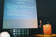
[Slide 18]

[Slide 19]

[Slide 20]

[Slide 21]

[Slide 22]

[Slide 23]
|
[Slide 18]
When I was watching the cathode luminescence from gallium nitride doped with zinc, the strength of the luminescence increased as time went on. I felt it mysterious and recorded it in detail - this is the data. The principle of cathode luminescence is that light emission is caused by stimulating the specimen using electron beam irradiation - similar to the cathode ray tube in a TV. So, this showed that the zinc-doped gallium nitride was changed by the electron beam irradiation.
[Slide 19]
I thought it interesting and made measurements of the electrical properties. But, at that time, I could not make a p-type crystal. I felt that it was impossible, as was expected. When I almost despaired of making the p-type crystal, I encountered a textbook. I was flicking through the textbook written by Phillips, "Bonds and bands in semiconductors", and happened to discover this picture.
This picture represents that magnesium is easier to use as a p-type acceptor dopant than the usually used zinc. I thought that it was a great hint and immediately changed the material from zinc to magnesium. Changing to magnesium alone was not effective in getting a p-type crystal, but, combining with the aforesaid electron irradiation, I succeeded in getting a p-type crystal for the first time.
[Slide 20]
We made the electrode only in a rudimentary way, compared with the presently developed process technique. Someone suspiciously said something about the measured voltage being somewhat higher than that for real p-n junction. But, I was very confident myself. Because I knew that the obtained film definitely showed p-type characteristics measured with Hall effect apparatus.
[Slide 21]
This is the example of the pattern delineated utilizing electron beam irradiation. This light emitting diode was fabricated so that the letter "M" was formed as the p-type region by electron beam irradiation. This p-type stripe pattern was made to confine the electric current to the narrow region for laser oscillation.
[Slide 22]
Next, I would like to introduce an example, not of success, but of failure. It is on the control of the emitted light wavelength. I succeeded in the crystal growth for gallium nitride. But, gallium nitride itself is the material to emit ultra-violet light. To emit blue light, indium must be added.
At the time, just after establishing the p-type gallium nitride fabrication, I started the experiment to add indium. But, I tried the experiments with the thought that it would be difficult, really hard - perhaps impossible. Because it was generally said that gallium nitride and indium nitride would not mix, like water and oil.
[Slide 23]
I worked hard with the master-course students. But, in nature of things, when you suspiciously try anything, you will fail in it. But, this was afterwards proved to be a great mistake. Later, for example, Professor Nakamura reported that the mixing experiment was possible and with very much brighter emission. Then, I retried the experiment again and it resulted in success.
|
|
|