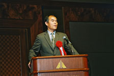
| Shuji Nakamura |
 |
|
|
 |
 |
|
My name is Nakamura. I am very grateful to be receiving this award. I had also prepared presentation materials but, as Professors Akasaki and Amano were going to make similar speeches, the Foundation asked me to make a speech without presentation materials, so that is what I will now do.
I was a corporate researcher. Professors Akasaki and Amano were researching at a university, but in my case I was at a company. Now I will talk about how I came to do research on light emitting devices (LED).
I was a graduate of Tokushima University - I graduated from a master's course at the University. I graduated from the electronics department, and after graduating, like most of the students in Japan, I wanted to join a big company. If we could enter big companies, we would be guaranteed lifetime employment as a salary man. Though I also intended to be a lifetime salary man, fate intervened, and it turned out that I needed to stay in Tokushima prefecture, for various private reasons.
Though I decided to stay in Tokushima, there was no company where I could use my electronics specialty, as Tokushima was a rural prefecture. I asked my supervising professor for an introduction to a company which was located in Tokushima prefecture, and I was introduced to Nichia Chemical Industry Co. Ltd (Nichia). Nichia's main products were fluorescent materials. Nichia was a chemical company in which fluorescent materials were developed and produced. My supervisor, Professor Tada at that time said, "You have to realize that you should resign yourself to being unable to apply your specialty, because the company is a chemical company and there is no job which uses an electronics specialty. You should work only thinking about looking after your family."
So I entered the company in such a frame of mind. Nichia was a company with 180 employees and yearly sales of 2-3 billion yen. The sales were all fluorescent materials. I was assigned to a development department when I entered the company. Though the name was the 'development department,' it consisted of section chief and two staff, as the company was such a minor enterprise. By chance, when I joined the department I was given as a research theme the development of crystal growth for the semiconductor gallium phosphate (GaP). This is a well-known crystal, which can be used for green and yellowish-green LEDs. I entered the world of LED development. At that time I felt extremely lucky, because I liked to study semiconductors. My professor said that "you should resign yourself to being unable to apply your specialty," but the actual situation was the opposite and I felt extremely lucky.
The company was, at that time, looking like it would go out of a business at any time. The previous year there had been an enforced lay-off, and it was a period in which the signature of your section chief was necessary when we wanted to get even small materials such as a pencil. I wondered whether the company was going to go out of business suddenly. However, the research theme, which I was ordered to tackle, was the crystal growth of the semiconductor GaP and I felt extremely lucky. I was entrusted with this research and worked alone. However we had little money to spend, and almost nothing, such as instruments, to do experiments with. Anyway I had to do this research, so I became hell-bent on doing experiments on the crystal growth.
At that time a horizontal Bridgeman method was used, and in this method it was necessary to put the raw materials inside a transparent quartz tube and so in order to do this I spent from morning to evening welding quartz tubes. Unlike a university, a company must produce manufactured goods. In a manufacturing company, making goods is the basic purpose. I of course was fond of reading technical books, but my work did not make progress as I was researching by myself. The chief urged me to start manufacturing something as soon as possible. So I spent almost every day welding quartz tubes, inserting raw materials and heating them in the furnace - where they would explode with a loud "bang." As I made the experiments in a company in the country, such troubles were permitted. If such explosions were to happen in the city, such operations would be shut down immediately.
I continued these kinds of developments for about 5 years - I researched GaP for 3 years and after that I did gallium arsenide (GaAs) for the next 3 years. In the research of GaAs, I did nothing but quartz welding. After I entered the company I did quartz welding from morning till evening almost every day. I was just a quartz-welding technician at that time! I couldn't imagine my present situation. At that time I thought that my whole life was over. I thought that I would end my life as a quartz-welding technician. As it turned out, I am now in a very different situation for one reason and another.
|
|
|