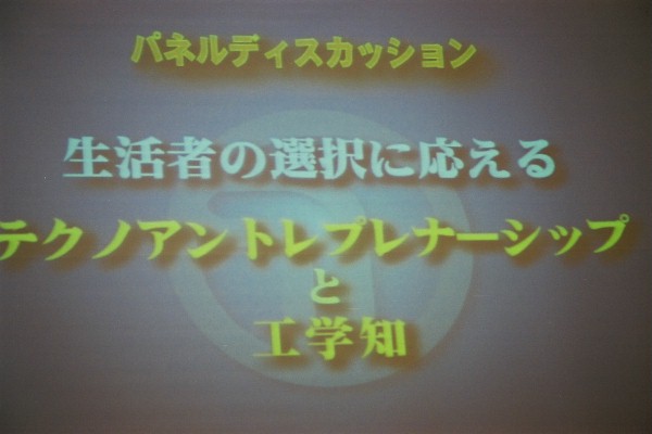
| Panel Discussion |
 |
|
|
 |
 |
|
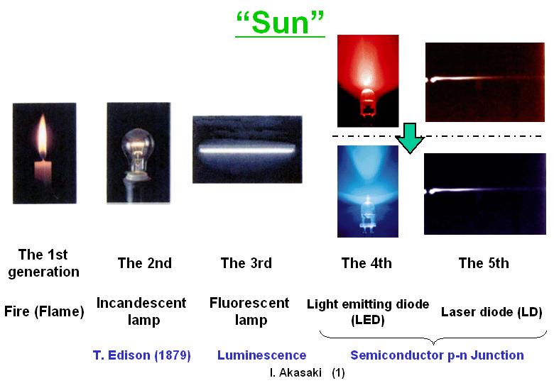
[Slide 1 (Akasaki)]
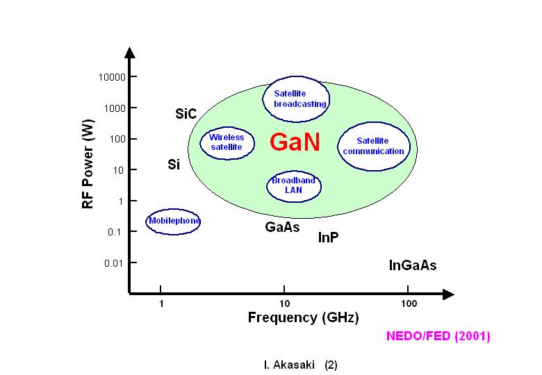
[Slide 2 (Akasaki)]
[Slide 3 (Akasaki)]
[Slide 4 (Akasaki)]
[Slide 5 (Akasaki)]
[Slide 1 (Amano)]
[Slide 2 (Amano)]
[Slide 3 (Amano)]
|
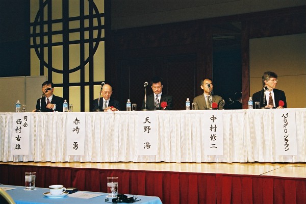
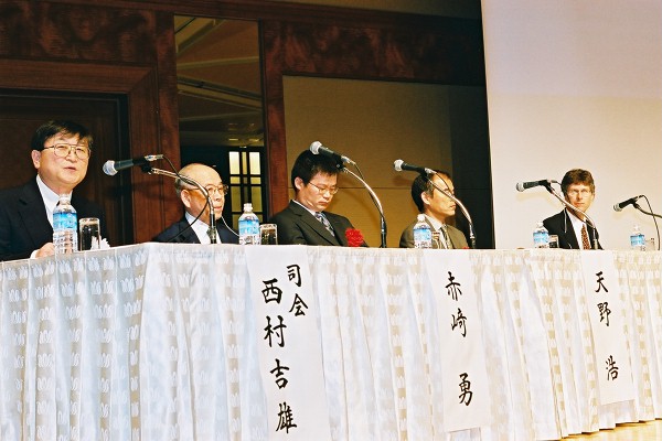
Nishimura:
Akasaki-san, please give your talk.
Akasaki:
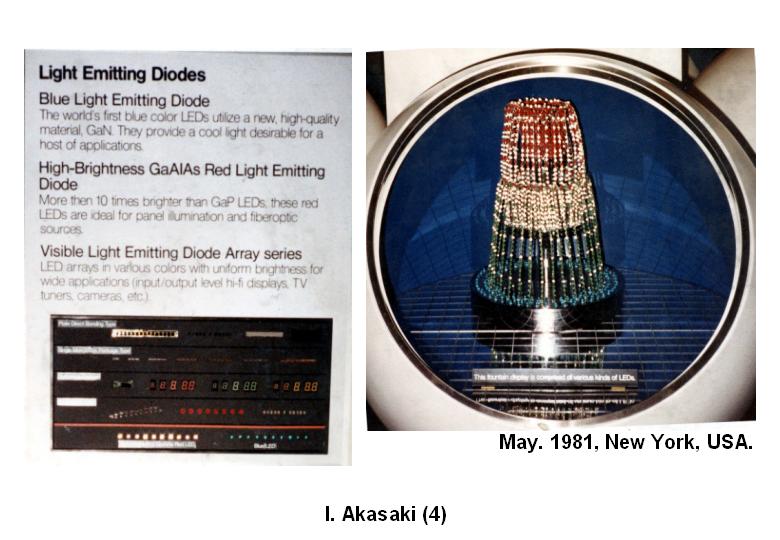
My name is Akasaki. We have just heard Nishimura-san explain the overall concept of Takeda Award, so I will now talk regarding my own case. As it is said that life has its origins in the interaction of water, air and sunlight, human beings have always adored the sun. This fascination with the eternal light of the sun, has led human beings to look for additional sources of light as slide 1. I think the first generation of light was flame or fire. The second generation was the incandescent lamp that was invented by Edison in 1879, using bamboo from Kyoto. After a long wait the third generation, luminescence or 'cold light,' appeared - light without heat. (In fact, in a fluorescent lamp the heated cathode does generates a little heat, but the light production itself does not generate heat). This feature - that no heat is generated - makes the 3rd generation technology very different from the 1st and 2nd generation lights. Additionally, until this 3rd generation, the need for a vacuum meant that the familiar 'bulb' shape had to be used. The light emitting diode and laser were invented when semiconductors came onto the scene in the latter half of the 20th century. The Takeda Award for Information and Electronics is being given to the invention of the blue light emitting diode and laser diode - developments that took a long time to make a success. New "knowledge" was added and introduced to the market by "entrepreneurship," to use Nishimura-san's phrase.
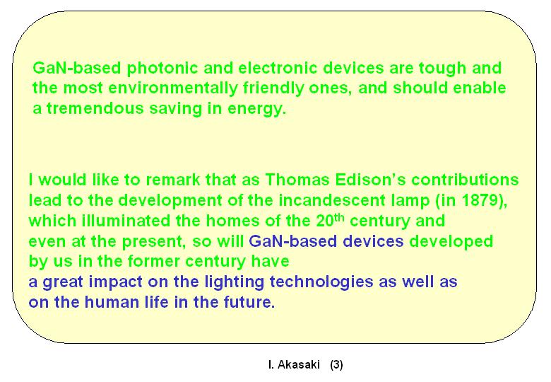
As I have mentioned this already in my remarks in the morning session, the invention of the blue light emitting device means that white light from a semiconductor device is now possible. The light emitting efficiency is currently better than incandescent bulb but worse than fluorescent lamp. I have confidence that, with the addition of new "knowledge," this efficiency will be improved and will replace the fluorescent lamp in the near future.
In the case of the laser diode, not only will it simply increase the recording density of optical storage devices, but new applications are also expected in fields such as biotechnology, medicine, and measurement.
I explained the optical applications in the morning session, but given that I have the time now I would like to add one additional point from a different perspective. I think the nitride semiconductor, or rather Gallium Nitride (GaN), shows promise as semiconductor material for electronic devices. The reason is that GaN has a large energy band gap, and so a large break down voltage can be realized even in fine scale applications. There are many other potential applications, such as high frequency devices. Transistors have a trade off - the higher the operating frequency, the lower the output power. New material development is needed to achieve high output power without decreasing operating frequency. Until today Silicon or Gallium Arsenide have been used. However, I believe a new transistor world based on Gallium Nitride is a real propsect. This slide 2 was made using NEDO and FED data - Gallium Nitride semiconductor is also a promising candidate to respond new application needs such as Broadband LAN or satellite communication.
This GaN is promising not only as a light emitting device but also as an electronic device in high frequency/high output power applications. However the most important strong point is that it is very tough and so can be used in hard operating environments as in slide 3. Nitride is the main constituent, so it is better for the environment than today's semiconductor materials. GaN has possibilities for both resource-saving and energy-saving applications.
I would like to make a final comment: When Thomas Edison switched on his incandescent bulb light, it had quite short life and was not very bright. The Blue light emitting devices which we invented at the end of 20th century, and which are recognized today by the Takeda Award's Information and Electronics section, will bring not only great advances in lighting applications, but also great value for human life. Thank you.
Nishimura:
Thank you very much, Akasaki-san. Amano-san, please give your talk.
Amano:
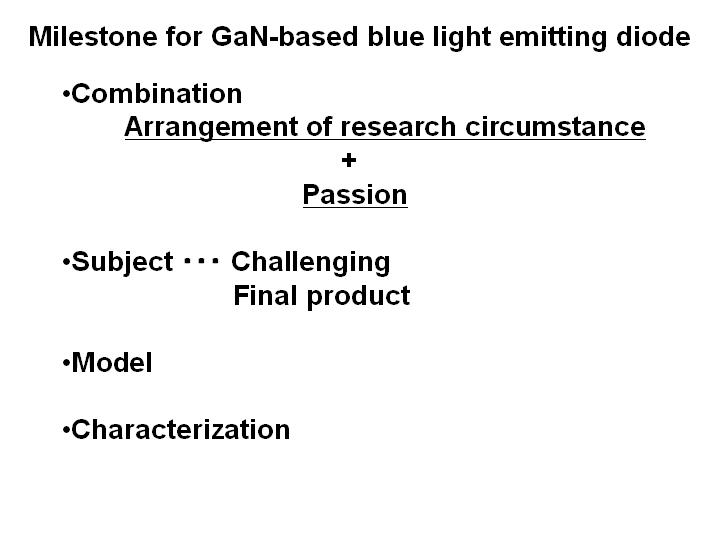
My name is Amano. Nishimura-san talked about "Techno-entrepreneurship" and "Kougakuchi" - engineering intellect and knowledge. It is easy to understand how techno-entrepreneurship is involved in the blue light emitting device because it is clear that if developed blue light emitting diodes can be of great use to people. Our job was, rather, how to realize itc how to create "Kougakuchi" - engineering intellect and knowledge.
I have drawn what I hope are some essential points from my experience and listed them in slide 1. If we have been successful in developing the blue light emitting diode, then the reason is that there is a great research environment that allows us to concentrate on our research work. Additionally, we had the passion to concentrate our efforts on achieving our goal. In order to have such passion, the target itself must be very attractive. As far as I at least was concerned, Blue light emitting diode development was the most attractive research theme. The development of a final product was in reach and its potential contribution to people was very clear. This is one reason I was able to make aggressive progress with my research.
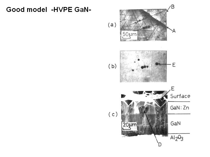
The thing that helped me make progress in my development work, and continue my research, was that there were existing models to use. We made crystals using the MOVPE method, but could only made crystals that were cloudy - like frosted glass. On the other hand, there was another method of making crystals called the HVPE. Crystal made by that method had many holes and many defects, but some areas of the crystal were beautiful - like stained glass as shown in slide 2. I set myself the target of producing such beautiful crystal using the MOVPE method and was able to drive myself to continue my research based on this target.
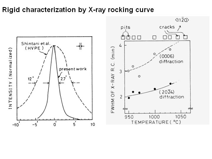
One other important point is that we had very detailed and accurate evaluation method. Crystal we made in initial stages was given a harsh evaluation if the quality was bad. At that time we were using a X-ray diffraction method to evaluate crystal quality. We can see inside of crystal exactly using this method. Finally, after much effort, we were able to make crystal that was superior even to that made using HVPE method as shown in slide 3. I think in doing that we were able to create one piece of "Kougakuchi" - engineering intellect and knowledge. I would like to conclude my brief talk there.
|
|
|