| Isamu Akasaki |
 |
|
|
 |
 |
|
[Slide 1]
[Slide 2]
[Slide 3]
[Slide 4]
[Slide 5]
[Slide 6]
[Slide 7]
|
[Slide 1]
Thank chairman for your introduction.
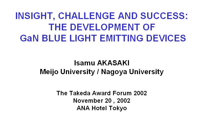
Ladies and gentlemen, I am Isamu Akasaki of Meijo University. The title of my speech is "The development of the gallium nitride blue light emitting devices -insight, challenge and success"
[Slide 2]
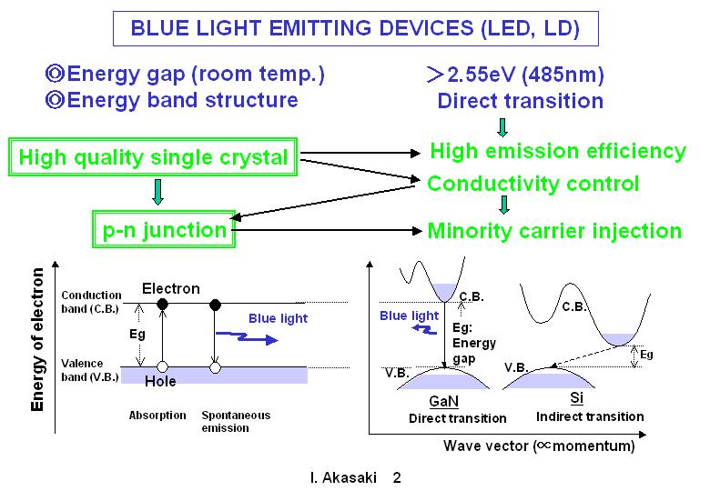
To create blue light emitting devices, as you know, it is essential to select a material, of which energy gap is above 2.6 eV. It is also necessary to use a semiconductor with direct transition type band structure, in which electron and hole momentum are equal, in order to conserve the momentum. In addition, a high quality single crystal of the material is required for high efficiency emission and, as I will mention later, for controlling the electric conduction. If these criteria are met - that is, the p-type and n-type conduction of the material can be controlled, meaning a p-n junction of the material can be realized and an injection of minority carriers becomes possible.
[Slide 3]
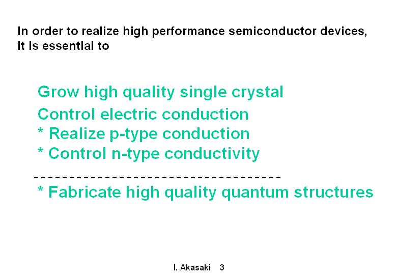
A further consideration is that a high quality quantum structure is required for high performance devices.
[Slide 4]
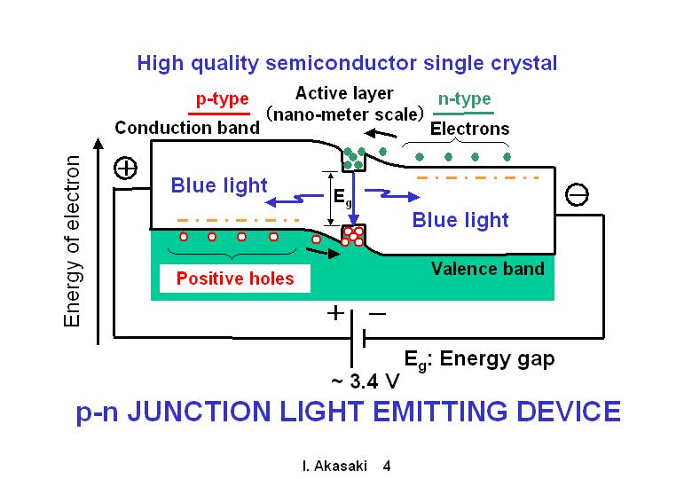
When a forward bias voltage which corresponds to the energy gap is applied to a p-n junction, electrons will be injected from the n-type region into the p-type region, and holes from the p-type region into the n-type region. The injected minority carriers recombine with majority carriers and light emission occurs. This device structure is very important, and is indispensable to high performance light emitting devices and other electronic devices.
[Slide 5]
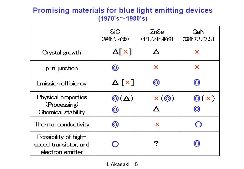
In the 1970s and 1980s, most of the researchers who intended to develop blue light emitting devices targeted these three materials. Of those, a p-n junction could only be obtained in silicon carbide (SiC). Accordingly, many researchers adopted SiC as their research material. The other researchers selected zinc selenide (ZnSe) or gallium nitride (GaN) as their material. Both materials were similar in the fact that a p-type conduction could not be realized. SiC is a semiconductor with indirect transition type band structure, and so strong light emission could not be expected and lasing would be impossible. On the other hand, ZnSe and GaN are semiconductors with direct transition type band structures, but a p-n junction could not be obtained. At this point, most of the researchers except for SiC people decided to select ZnSe as the material. One reason for the selection of ZnSe is that growth of a single crystal is not quite as difficult as with GaN, although growth of a single crystal is difficult in both materials. The other reason is that ZnSe is softer and easier to process than GaN. GaN is very hard and very difficult to process. Moreover GaN has a wide energy gap, and so it was assumed that creating a p-type material would be more difficult in GaN than in ZnSe. However, GaN is very hard and tough, while showing good thermal conductivity. If problems mentioned above could be resolved, the material would have great potential for new electronic devices. Although I felt these would be very difficult problems to solve, I accepted the challenge of GaN, which was deemed difficult to fabricate into a p-n junction type blue light emitting device.
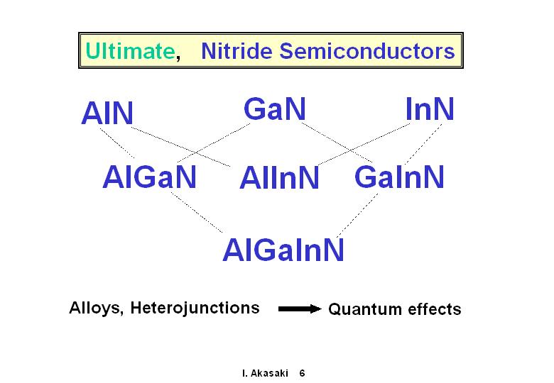
[Slide 6]
GaN has two brothers - aluminum nitride (AlN) is its elder brother and indium nitride (InN) is its younger brother. We can combine these to get mixed materials, called alloys or mixed crystals, which show in-between properties. If we use these materials to fabricate a p-n junction, the junction is called a heterojunction and shows good characteristics in increasing carrier injection efficiency and so on. Also if we fabricate nanostructure devices using these materials, we can get quantum effect devices.
[Slide 7]
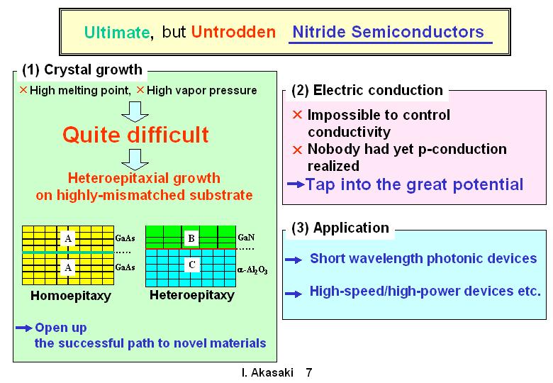
In that sense, it can be said that these GaN-based nitrides are the ultimate semiconductors, but it is quite difficult to produce. From the perspective of crystal growth, GaN has a high melting point that is still not accurately known.@Further the vapor pressure of nitrogen in nitrides is quite high. So, it is very difficult to grow large single crystals. In such situations, the method of epitaxial crystal growth is often used. The word "epitaxy "is Greek and means that the crystal grows in accordance with the substrate crystal axis. Growing silicon (Si) on Si and gallium arsenide (GaAs) on GaAs is called" homoepitaxy "and in principle there should be no interfacial energy. However the situation is quite different in the case of GaN on sapphire - large interfacial energy exists. This is a very thorny problem. In addition, electric conduction could not be controlled. Moreover, no one had realized p-type GaN, which is essential for making semiconductor devices. At that time it was even said to be theoretically impossible to make p-type GaN. However, if I could solve these problems for instance the heteroepitaxial problem - then I could develop heteroepitaxial materials that would pave the way for entirely new electronic materials. I figured that if I could control the electric conduction of GaN, I could unlock the door to many practical applications using GaN-based nitride semiconductors. I believed that solving the above problems was a challenging and worthwhile research theme. Today I will talk about two typical examples of the successes - blue light emitting devices and ultra high speed/high power transistors.
|
|
|