| Isamu Akasaki |
 |
|
|
 |
 |
|
[Slide 21]
[Slide 22]
[Slide 23]
[Slide 24]
[Slide 25]
[Slide 26]
[Slide 27]
|
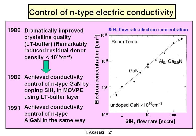
[Slide 21]
With this discovery, I was confident that all of the problems were solved. However another problem arose - due to the decreasing density of residual donors and the good crystallinity, the resistivity of the n-type GaN increased. In order to fabricate practical electronic devices, the resistivity must be variable from very low to very high. We found that Si behaved as a donor in GaN and, still using the LT- buffer layer, we succeeded in doping Si into GaN while maintaining good crystallinity. I am showing here in this slide the increasing n-type conductivity and conversely the decreasing resistivity over wide range. The conductivity control of n-type nitrides was also achieved in the same year as the discovery of p type conduction- 1989.
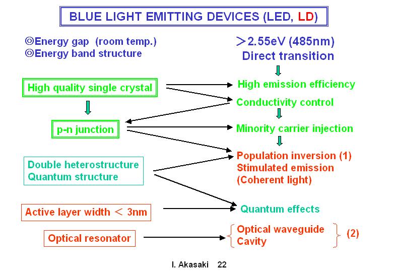
[Slide 22]
Concerning the development of the laser diode (LD), the details in the upper part of slide 22 are same as for the LED, but as you know, in order to make an LD stimulated emission must be induced.
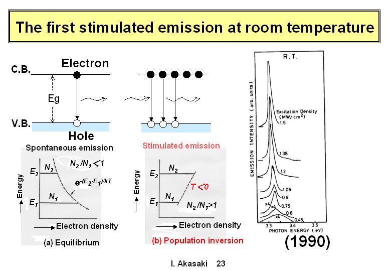
[Slide 23]
Normally, low-energy electrons dominate the electron distribution. However, for stimulated emission the population of high-energy electrons should exceed low- energy ones. This situation can be attained by excitation. This is called "population inversion", and results in a negative temperature according to the Boltzmann distribution. In this situation stimulated emission occurs and this emission is coherent light which is in phase. By amplifying this stimulated emission, a laser oscillation will occur. In 1990, we were successful in making a room temperature stimulated emission, for the first time, with the high quality GaN film grown with the LT-buffer layer.
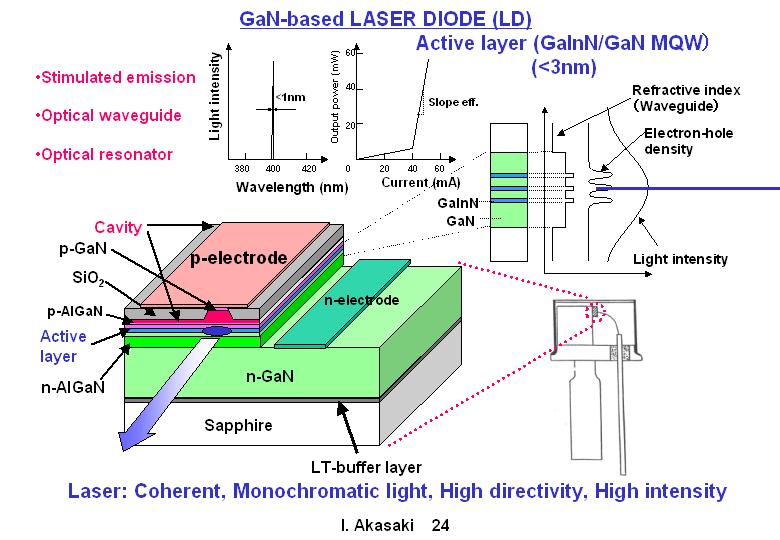
[Slide 24]
The LD characteristics are shown here in this slide, in which the transverse axis is applied current and vertical axis is light output. The light output increases abruptly as the applied current exceeds a certain current. This current is called the threshold current.
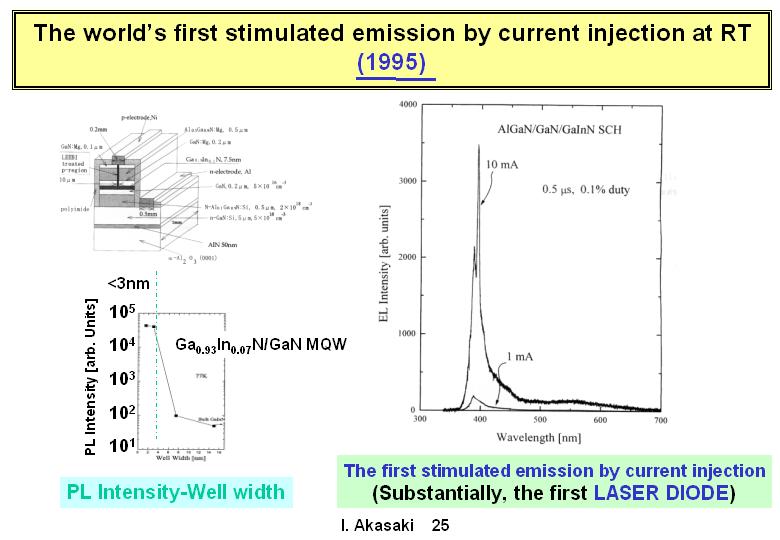
[Slide 25]
Since the work described earlier, we have decreasing the threshold power by one tenth each year. We found that the intensity of a band-edge emission from multi-quantum wells increased dramatically (about 3 orders of magnitude), when each well width was under 3 nm. Although it was later on (in 1997) that we proved that this phenomenon is related to the quantum effect, in 1995 we used it to demonstrate a successful stimulated emission by current injection from GaN-based quantum well structure, for the first time, worldwide. It was the beginning of nitride based LDs, although this device had a short lifespan.
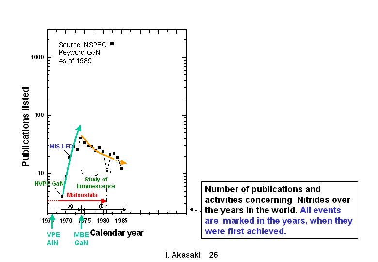
[Slide 26]
Although the numbers of publications were decreasing rapidly@till the mid- 1980s, as shown in this slide,
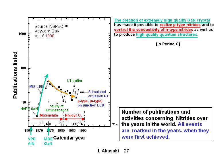
[Slide 27]
This was the same time period when I was at Nagoya University. The crystallinity was improved drastically, the p-type conduction was realized, the conductivity control of n-type nitrides was achieved and p-n junction blue LED was also developed. Moreover, the room temperature stimulated emission was made possible.
|
|
|