| Isamu Akasaki |
 |
|
|
 |
 |
|
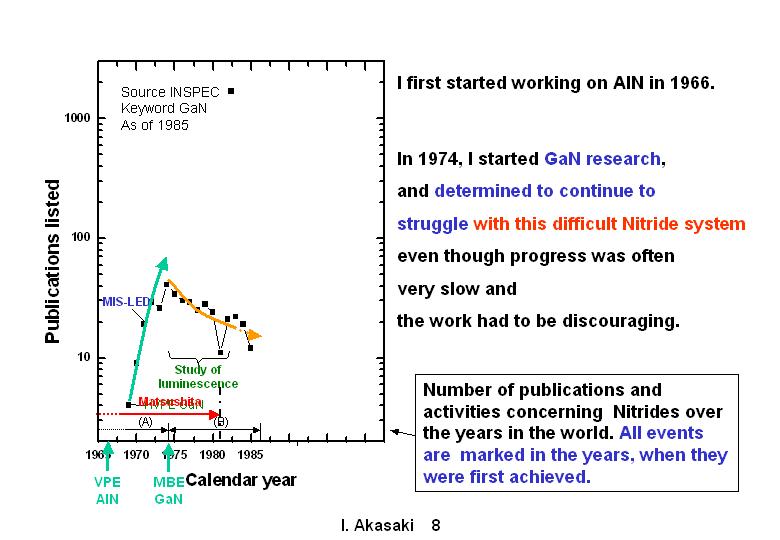
[Slide 8]
[Slide 9]
[Slide 10]
[Slide 11]
[Slide 12]
|
[Slide 8]
I will explain the status of the research in the world - this slide shows the number of publications on nitride semiconductors worldwide, by year. Note that the vertical axis uses a logarithmic scale. In 1969 a small single crystal of GaN was grown first, and in 1971 a blue-green MIS type light emitting diode (LED) was fabricated, although the light intensity was low. The research activity increased abruptly at this point.
However, in spite of great efforts by researchers around the world, it has been quite difficult to grow a high quality GaN single crystal with flat surface free from cracks. Moreover, as-grown GaN contains high density residual donors and has strong n-type conductivity. Furthermore, p-type GaN had never been realized. Thus, most researchers in the world gave up researching GaN.
[Slide 9]
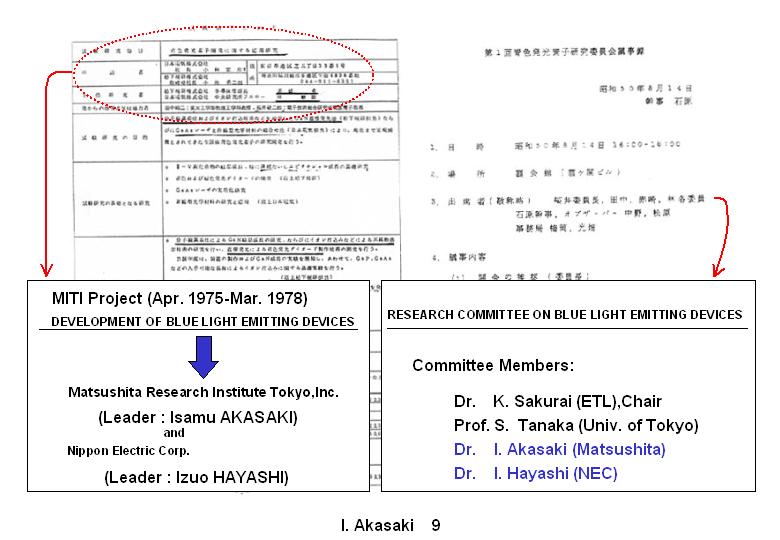
At that time I was at Matsushita Research Institute Tokyo, Inc. (MRIT), and I was very interested in nitride semiconductors. I grew AlN by using chemical vapor deposition (CVD), and I was investigating the optical properties of AlN. We found Reststrahlen band in AlN first. However, the energy gap of AlN is so large that AlN is an insulator and doesn't allow the flow of electric current. Then I started research on GaN in 1973, and in 1974 I succeeded in growing a GaN single crystal film first by using molecular beam epitaxy (MBE). I took the new data on GaN single crystal film grown by the MBE method, to MITI to apply for a big project. At that time Dr. Hayashi in NEC applied for the project to realize a blue light emitting device using second harmonic generation of GaAs laser. At the Agency of Industrial Science and Technology of the day, there was a very discerning officer who judged that these two proposals were very important, though for each of them the goal would be very difficult to attain. The officer proposed a joint project, though this would be very difficult. The three-year project started in April, 1975. Because Dr. Hayashi and I were both in private companies the late Dr. Kenjiro Sakurai of the Eletrotechnical Laboratory, and Prof. Shoji Tanaka of the University of Tokyo, joined the project as committee members and the research group for blue light emitting devices started with four members. I think that back then the project was very unique even from an international perspective.
[Slide 10]
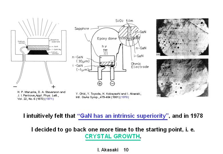
After three years of research, my group had performed selective area crystal growth of GaN, which I think it was rare at that time. In the MIS diode so far, the electrodes had to be extruded from a very thin layer, but now we could make a sufficient area of n+region in the insulating layer by using the selective area crystal growth to easily extrude the electrode. By using this technology several thousand LED samples were manufactured in trial production, but mass production was not yet possible. The reason why the devices were not suitable for mass production because, even though great improvements in quality had been made, the crystal had many cracks and pits as shown here. I investigated this film in detail, using fluorescent microscopy and realized that there were very clean areas here and there, and so I developed a gut feeling for the inherent quality of GaN. I was confident that I would obtain an excellent crystal film with a mirror surface, if I somehow could just expand this small clean area to full wafer scale. So I decided to return one more time to the starting point, which is crystal growth.
[Slide 11]
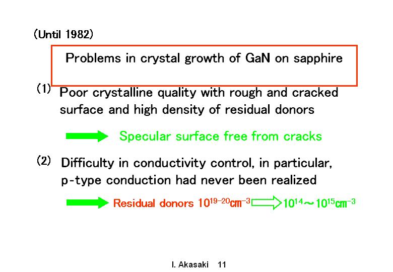
In summary, one problem was the poor crystallinity of the GaN film and the other problem was that the film contained high density of donor impurites. I believed that these two problems were closely connected each other, and should be solved at the same time. Concerning the first problem, I thought that the film surface had to be flat just like a mirror. I also wanted to decrease the residual donor density in the film from around 1019 cm-3 to below 1015 cm-3.
[Slide 12]
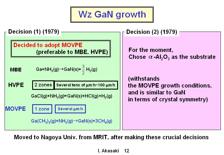
By the way, the most important factors in a crystal growth are@selecting the method of crystal growth@and selecting the growth conditions. After four years and many of trials, I concluded that MBE was not suitable for the growth of nitrides@despite being one of the best methods for crystal growthA because of the high vapor pressure of nitrogen in nitrides . The other method, hydride vapor phase epitaxy (HVPE), had been widely adopted for crystal growth but was also not suitable for the growth of nitrides. The HVPE method uses two separate reaction zones at different temperatures, and the crystal growth rate is too high. The other reason, which I do not describe in detail here, is that the chemical reaction would be a reversible reaction, which means that there is a chance to etch the grown crystal film. Therefore, I selected metalorganic chemical vapor deposition (MOCVD, or MOVPE) as the growth method (Decision -(1)), though this method rarely employed at that time. In this method the crystal grows in one temperature zone, and the growth rate of crystal lies between the rates of the preceding two methods. The other important matter is that in this method, as is shown here with an arrow, the chemical reaction is irreversible and the reverse reaction never occurs. So I thought this method would be considerably better than others in terms of controlling crystal growth. After the selection of the method for crystal growth, the next item was what kind of substrate I should select. At that time Si, GaAs and the like could be produced in good single crystals - but for growing nitrides the growth would have to be done at a very high temperature, over 1000 , in a highly reductive ammonia atmosphere, and the substrate would have to be able to endure such conditions. Thinking from the point of view of endurance and crystal symmetry, I chose sapphire, which had the same, three-fold symmetry as the nitrides (Decision-(2)). I selected sapphire provisionally while believing that a better substrate would appear in the future. After I made (in 1979) these two important decisions, I returned to Nagoya University.
|
|
|