| Isamu Akasaki |
 |
|
|
 |
 |
|
[Slide 13]
[Slide 14]
[Slide 15]
[Slide 16]
[Slide 17]
[Slide 18]
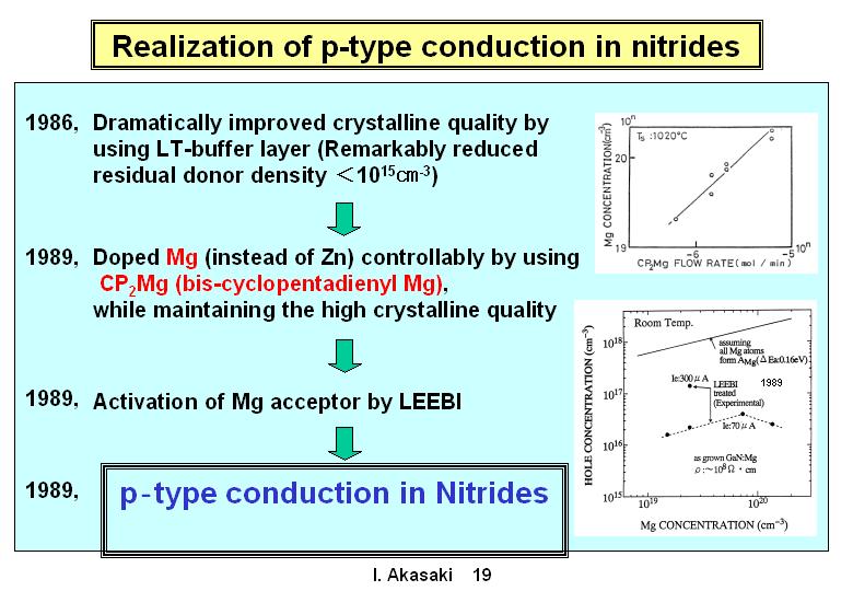
[Slide 19]
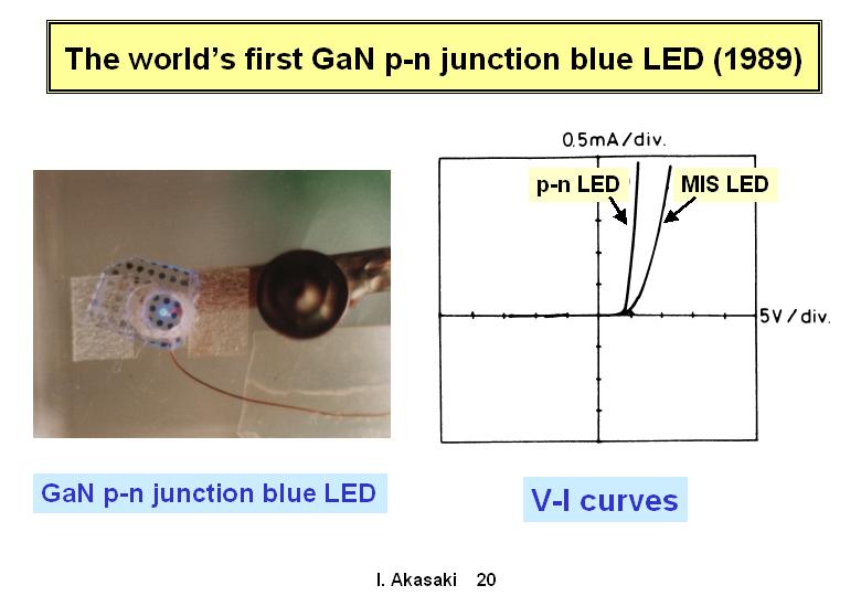
[Slide 20]
|
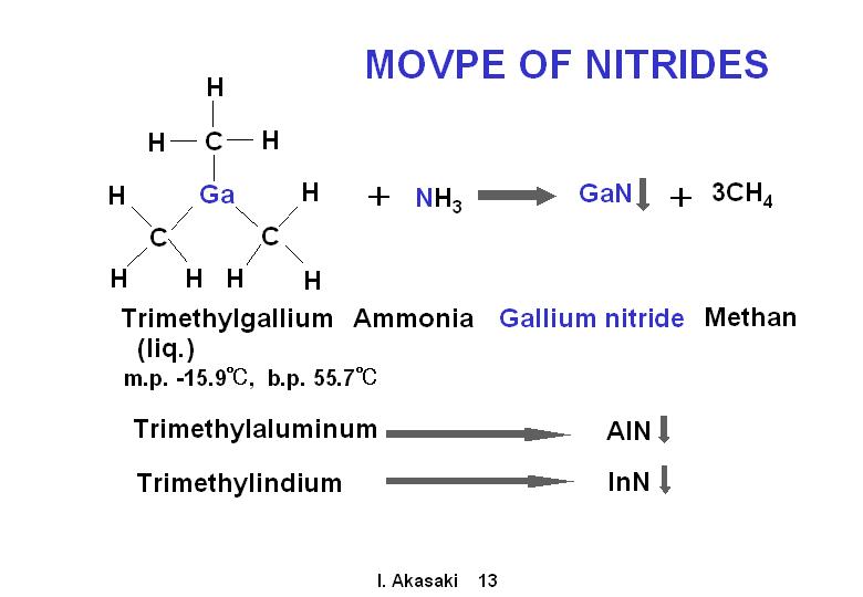
[Slide 13]
By using MOCVD, GaN, AlN or InN could be made by replacing this gallium (Ga) with aluminum (Al) or with indium (In). Also mixed nitride crystals could be obtained by appropriately mixing these materials, as shown here.
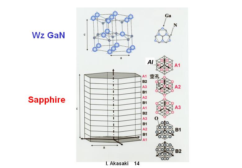
[Slide 14]
Concerning the sapphire substrate, the critical factor is that it has the same three-fold symmetry as the nitride crystals. But if you compare the actual dimensions of these crystals, the two differ greatly. This is not just true in terms of the lattice constant value; there are also big differences in other physical properties.
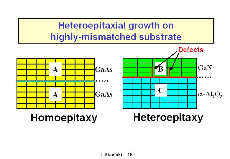
[Slide 15]
Therefore it can be assumed that a very large number of defects are introduced at the interface. This is caused by a large interfacial energy between sapphire and nitrides.
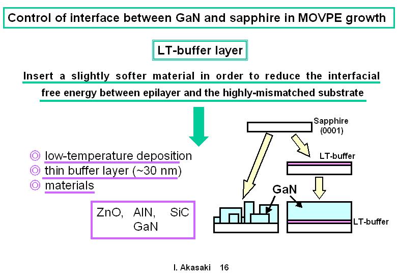
[Slide 16]
In order to overcome this problemc this was around 1982c I came up with the idea of inserting some kind of soft material which should be deposited at low temperatures in case of crystal growth between the two. At the same time, I considered that if the intermediate material were too thick, it would mask the 'information' such as crystal symmetry of the substrate. Therefore, I thought that an overly thick layer was not suitable and it should be kept thinB I named this intermediate layer the "low-temperature deposited (LT-) buffer layer", based on the concept of the thin buffer layer. At that time I had four candidates for materials. Because I could not test the four materials simultaneously, I asked a researcher at Yamanashi University to test ZnO, and a researcher at Kyoto University to test SiC. As I mentioned earlier, I already had experience with depositing AlN crystals, so I decided to test AlN first as a buffer layer at Nagoya University.
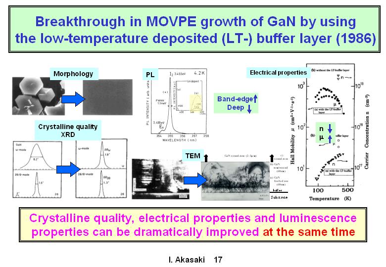
[Slide 17]
My co-recipient Dr Amano, after an enormous effort and many setbacks, finally identified the best buffering conditions. These are the photographs of the grown film. Without the buffer layer, you can see that the GaN layer is very rough. While with the buffer layer, the photograph shows a very smooth surface. The X-ray diffraction profile of the GaN grown with the buffer layer became much narrower. Luminescence properties, which had so far given a dirty yellow band, improved dramatically and showed only strong band-edge emission. In terms of electrical properties, the reduction of residual donors by four orders of magnitude led to a dramatic increase in the freedom of electron movement, and hence an increase in electron mobility. This transmission electron micrograph, though it is not so clear, reveals that lattice distortions are concentrated near the buffer layer and the upper epilayer is quite smooth. In summary, by using the LT- buffer layer, all of the properties of GaN, crystallinity, electrical properties and luminescence properties - which are all equally vital - have been dramatically improved simultaneously.
[Slide 18]
You can see that there are clear differences between this slide and the preceding slide.
[Slide 19]
At this point, I thought that it would be easy to obtain p-type GaN. In order to realize p-type conduction, it is first necessary to decrease the density of residual donors to at least 1015cm-3, and then under these conditions the crystal should be doped with acceptor impurities. As zinc (Zn) was commonly used at that time as a blue luminescence center, we started with Zn. However, p-type conduction had never been realized by doping Zn as an acceptor impurity. We noticed that magnesium (Mg) has smaller activation energy than Zn. We decided to change Zn with Mg and to adopt a metalorganic compound bis-cyclopentadienyl Mg (CP2Mg) as a dopant. In 1989, Mr. Kito a postgraduate student succeeded to dope Mg into GaN using CP2 Mg. Then, we realized, for the first time, p-type GaN with low energy electron irradiation on such a high quality Mg-doped GaN grown with the LT-buffer layer in 1989.Although I could comment on this too, I think that Dr. Amano will probably talk about this later.
[Slide 20]
At exactly the same time we succeeded in realizing a p-n junction type GaN blue/UV LED. This slide shows the photograph that I presented at the Los Angeles conference - all of the black spots are p-n junction blue light emitting diodes, and just one of them has an applied voltage and is lighting. Although this photograph is not very clear, I would like to point out that this GaN layer grown on the sapphire substrate has no cracks and looks entirely transparent and colorless. The voltage-current characteristic has been improved dramatically, and of course the above mentioned GaN layer was confirmed as p-type conduction by using Hall effect measurement.
|
|
|